
The believer who stopped promising
Bob Mumgaard spent a decade telling the world fusion was almost here. Now the magnets are arriving on schedule, and the most careful thing he says is the date he won't give you.
Douglas Yu spent thirty-one years inventing the way the world's chips are stacked, then retired. The trouble is the world stacked itself around him, and now it cannot quite let him leave.
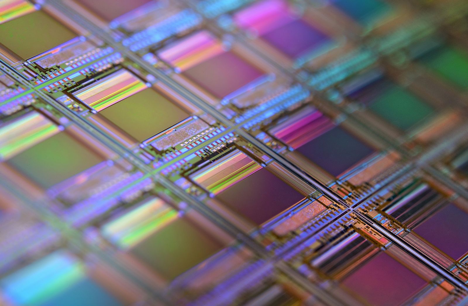
Photograph: Laura Ockel / Unsplash
The thing about the man who taught the world to stack its chips is that he no longer has to go to the office, and yet the office keeps arriving at him. In July of last year Dr. Chen-Hua Douglas Yu walked out of TSMC for the last time as an employee, after thirty-one years, the company's sole Distinguished Fellow, the engineer his colleagues had taken to calling the Final Knight. Retirement, in the ordinary sense of the word. Ten months later, in May, MediaTek announced it had brought him back — part-time, an adviser, helping a rival explore the very technology he had spent half a working lifetime inventing inside the building across town. He had left the room. The room followed him out the door.
You can read the whole of him in that gap between the leaving and the not-quite-leaving. Yu is the person almost no one outside the trade can name and almost no one inside it can do without — the author of the unglamorous middle step, the part of the chip nobody photographs. When Nvidia ships an AI accelerator, when a data center the size of a town hums into life to train a model, the silicon at the heart of it has been through a process he is more responsible for than any single living engineer. It is called CoWoS. It is, in plain terms, the art of gluing the future together so precisely that it behaves as one thing. And the man who perfected the glue spent his career being told the glue did not matter.
To understand why Yu is interesting you have to understand what he chose, which is the part of the work the industry spent decades treating as a chore. For most of the history of semiconductors the romance lived in the transistor — smaller, faster, denser, the relentless shrink that Gordon Moore turned into a law and a religion. Packaging was what happened afterward. You made the brilliant chip, and then somebody put it in a box. The box was an afterthought, a cost line, a problem for the people who could not get into the transistor priesthood.
Yu became the man who made the box matter more than almost anything. His full name is Chen-Hua Douglas Yu; he holds a master's in materials science from National Tsing Hua University and a doctorate from his time in the United States, and before TSMC he spent the years from 1987 to 1994 at AT&T Bell Labs in New Jersey, a member of technical staff working on the sub-micron processes that were then the bleeding edge. He joined TSMC in 1994, the year the company was still better known for making other people's designs than for inventing anything itself. His first great contribution was not packaging at all: he led the move to copper interconnects and low-k dielectric at the 0.13-micron node, the wiring change that, around 2003, helped TSMC pull ahead of the field. It is the kind of accomplishment that would have been a whole career for anyone else. For Yu it was a warm-up.
He chose the part of the chip nobody photographs, and then made it the part the whole industry could not ship without.
What he turned to next was the thing he is remembered for: wafer-level system integration, the idea that you could stop treating the package as a box and start treating it as architecture. If you could not shrink the transistor much further — and by the late 2000s the shrink was getting harder, slower, more expensive every node — then you could win by how cleverly you joined chips together. Put a processor and a stack of high-bandwidth memory side by side on a slice of silicon, the interposer, and wire them with connections so fine and so short that the seam between them all but disappears. Chip on Wafer on Substrate. CoWoS. He gave it the least poetic name imaginable and then spent years defending it from people who thought it was a distraction.
This is the part of the story that gets sanded smooth in the retellings, and it is the part that actually tells you who he is. CoWoS was not an obvious bet. For most of the 2010s it was a niche — exotic, expensive, useful for a handful of high-end networking and graphics parts and not much else. The volume business was elsewhere. The internal logic of a foundry rewards the technology that fills the fab, and for years CoWoS did not fill the fab. Yu kept building it anyway, refining the interposer, shrinking the gaps, adding the derivatives — Integrated Fan-Out, which arrived in 2016 inside the Apple A10 that powered the iPhone 7 and proved fan-out could ship in the hundreds of millions; then SoIC, the move from packaging chips side by side to stacking them in the third dimension.
He was, in other words, ready before the world was. When the generative-AI boom arrived and every large model on earth suddenly needed processors lashed to towers of memory, there turned out to be exactly one company with a mature, high-yield way to do it at scale, and exactly one body of work it rested on. The bottleneck of the AI era was not the transistor. It was the packaging. It was CoWoS. The capacity that Nvidia and the cloud giants have spent the past two years fighting over — that, this past April, sent Nvidia scrambling to lock down TSMC's advanced-packaging lines — is the capacity for the thing Yu built in the lean years when no one was watching.
There is a particular kind of vindication in that, and it would be easy to write him as the prophet who was right all along. But the people who worked with him describe something quieter and more stubborn than vision. They describe a man who simply did not accept that the package was an afterthought, and who kept saying so in rooms full of people who had decided otherwise, for fifteen years, until the rooms changed their minds. That is not prophecy. That is the refusal to be bored by the unglamorous problem.
The recognition, when it came, came in a flood, and it came late in the way these things tend to. He was made an IEEE Fellow in 2013. Taiwan gave him its Presidential Science Prize in 2017. The IEEE handed him its Outstanding Manufacturing Technology Award in 2018. TSMC named him its sole Distinguished Fellow in 2021 — a designation invented, more or less, to describe a person the existing titles did not fit. In 2024 the Academia Sinica, Taiwan's most rarefied scholarly body, elected him an academician, the kind of honor usually reserved for theorists, not for the engineer who figured out how to make the gluing step yield.
He holds, by the count that circulates in the trade, more than eighteen hundred patents. Inside TSMC the legend hardened into a nickname: the Final Knight, the last of the Six Knights of R&D, the small group of engineers — among them the lithography pioneer Burn Lin — credited with turning a contract manufacturer into the most strategically important company on the planet. The framing is heroic and a little mythological, the sort of thing a company tells about itself. It is also, in his case, not far wrong.
He was ready before the world was. The bottleneck of the AI era turned out to be the thing he had quietly built in the years nobody was watching.
And here is the tell, the small thing that does not fit the monument. A man with eighteen hundred patents and every honor his field can confer, the engineer whose work underwrites a multi-trillion-dollar boom, retired at the height of that boom's hunger for exactly what he made. He could have disappeared into the most decorated retirement in the history of his profession. He lasted ten months.
In early May, MediaTek — TSMC's neighbor in Hsinchu, a designer of chips rather than a maker of them, now pushing hard into the AI-accelerator business it expects to be worth billions by 2027 — said it had appointed Yu as a part-time adviser. The company's language was careful and corporate: it looked forward, it said, to leveraging his extensive industry experience and technical expertise to support its exploration and roadmap planning for future advanced packaging technologies. Read it twice and you can hear what it is not quite saying. The man who built the moat is now consulting for the people standing on the far bank.
It would be a mistake to make this dramatic. He is an adviser, part-time, to a firm that does not compete with TSMC where TSMC is strongest; the chip world is small and incestuous and these threads cross constantly. But it is worth sitting with the shape of the choice. A person who has won everything, who owes the industry nothing, who could spend the rest of his life as the grand old man of a technology that finally got its due — and who instead went back to the bench, in a quieter building, to think about what comes after the thing he is already famous for. Chiplets. The next dimension of stacking. The packaging problem after this packaging problem.
You meet, sometimes, the person who built the cathedral and then cannot stop noticing where the next one should go. The honors say the work is finished — the academician's seat, the Distinguished Fellow's title, the retirement. The man's actual behavior says it never is, that the interesting question is always the one just past the edge of what currently works, and that being right twenty years ago about the unglamorous middle step is not a place to rest but a reason to do it again. He spent thirty-one years insisting the seam mattered. The world finally agreed. And the moment it did, he went looking for the next seam.
There is a photograph that should exist and probably does not: Douglas Yu, retired, decorated, free, sitting in an unfamiliar office in front of a whiteboard that is not his company's, sketching the way you might join two pieces of silicon that no one yet needs joined. The future, by then, will have been glued together so seamlessly that you will never see his hand in it. That was always the point. The best packaging is the kind you forget is there.